Affected firmware: All version below v4.2.2 including btc-only
Fixed in: v5.0.0
I’ve become hooked on the adrenaline rush of finding security vulnerabilities in hardware wallets. Now this might sound super lame, but don’t knock it till you try it #nerd_rush. Bitcoin hardware wallets are a great target because virtually all attacks are significant including physical attacks. And all devices are vulnerable to some level of physical attack it is just a question of how much time and money the attacker wants to spend. Also, even single device attacks that cost thousands of dollars can be significant because it is common for people to store many multiples of this on hardware wallets. The password brute force attack discussed here however is relatively low cost (~$100), but a little slow (~5 sec/guess).
Introduction
The BitBox02 is a new hardware wallet from Shift CryptoSecurity and I found it to be a very professionally designed device with good usability. The BitBox02 uses the ATSAMD51 from Microchip, a general-purpose Cortex M4 MCU, along with an ATECC608A secure element from Microchip (big chip and small chip in the pictures respectively). My initial interest in the BitBox02 was focused on finding an error in their usage of the secure element. So, I started by using a sophisticated tool to remove the epoxy to expose the secure element and the bus.
But after reviewing the code for an hour or two I was disappointed to not find any errors. I started to get worried my needed nerd rush was going to be left unsatisfied. Family life really limits the amount of time I can spend so I needed to find something soon. After a couple more hours I finally noticed something that had some potential, a possible side channel attack on the password entry check.
To many less technical people lots of these attacks sound unintelligible and seem more like magic than engineering, so I’m going to try and simplify my descriptions here to make this document more useful to the masses. Side channel attacks generally refer to any way a system leaks information outside of its normal behavior. To make this more understandable for you normies let me first give you an example of a real-world brain teaser problem that is very analogous.
Problem: There is a room with three light bulbs and a closed door, you are outside. There are no windows and the door seals tight such that no light can exit. Outside the room there are three light switches, one for each bulb. You can freely manipulate the switches, but you can only open the door to the room one time. How can you figure out which switch goes to which bulb?
Take a second and see if you can come up with a solution… Hint, you need to preform a side channel attack.
The normal behavior of information exchange with a light bulb is: Switch on - light bulb emits light, Switch off - light bulb is dark. But like hardware wallets light bulbs are physical devices so there are many other properties. For example, think about how can you tell if an installed light bulb is brand new or “old”? Well there are probably many ways, but you could just look at it and see if it has dust on it. Or maybe you can see a date code printed on it and it is very old. Any normie can figure out these methods because light bulbs are something everyone is familiar with. This is exactly the familiarity researchers have with embedded hardware. Most attacks usually aren’t that “hard” but are more like the previous brain teaser for embedded systems, when you find the solution/attack it seems simple and obvious.
Light bulbs leak information about their previous state in a very strong way. If you are familiar with incandescent bulbs you are very familiar with this property. A light bulb that was previously on, but is now off, will stay very hot for some time. So to determine the state of three bulbs you turn two on and one off and wait some time. Then before you enter the room you turn one of the two on, off. Now when you enter the room one will be on and two will be off, but one of the off bulbs will be hot. Now you can match them to the controlling switch.
In embedded systems power consumption is also an important side channel. We can use real time power consumption measurements to see inside the chip and what it is doing. Everything a chip does turns on different numbers of transistors inside the chip and additionally those route power to other places in the chip at different times. Looking at the power can very accurately tell you in real time what the chip is doing. Now let’s review some security features in the BitBox02 and hopefully the method of attack will make a little more sense when you hear it now that you have some foundation to build from.
BitBox02 Security
The BitBox02 uses a workflow similar to many other hardware wallets. The user sets up the device for the first time and the device generates a “seed” that is a root key to derive all the bitcoin private keys. Next you create a device password to unlock access to the seed for signing bitcoin transactions. This flow is common across many devices. Where the different wallet manufactures differentiate their security is how they protect the seed from extraction and unauthorized usage.
The BitBox02 uses a secure element (SE) to help increase the system’s security level, but it is important to understand exactly how it is using this chip to help. If a secure element is misused it can make your security weaker than just using the MCU by itself. One thing to note about the ATECCx08A (SE) is it doesn’t actually support the bitcoin cryptography (this is not a problem). All the bitcoin related cryptography is done in the MCU in software. The SE is just being used to protect some of the key material used to encrypt the bitcoin seed which is stored in the MCU flash. Shift did a good job with the system architecture in how the key material is divided up. They use the user password + MCU secret + SE secret to create the final secret which authenticates and decrypts the bitcoin seed stored on the MCU. This means a BitBox02 attacker needs to recover all these keys to decrypt the seed directly (well at least the MCU and SE, the user key can typically be brute forced). Not storing everything in the SE is especially important because even though an SE is designed to be strong against physical attacks, no device is immune. Including the MCU to store one of the keys is effectively adding another layer of security that is independent from the SE (defense-in-depth). Having additional layers of protection is important, Shift does this in another area as well which helps mitigate my attack.
Another important security function of wallets is limiting the number of guesses that an attacker can make to discover the user’s password. The BitBox02 uses a limit of 10 guesses enforced by software. If you exceed 10 guesses the wallet wipes out the “keys” on the secure element (SE). This permanently eliminate the attacker’s ability to recover the seed. This limit is important because humans often choose weak passwords. Another thing that compounds this weak human password issue is that the BitBox02 has the user enter their password on the BitBox02 itself. I believe this causes users to use less complex passwords just because the process of entering it is “slow”. I am a fan of the new capacitive touch UI for the BitBox02 and it's better than other competitors, but it isn’t the same as a keyboard. This should cause shorter passwords than normal on average. Using a PC or phone paired with the device is another option for making longer/stronger user passwords, but this introduces more risk an attacker can recover the entire password directly with malware on one of those devices. In my opinion it is best to enter the password directly on the device itself, but the wallet designer needs to be aware users will choose shorter passwords and I don’t believe asking the user to have a “strong” password helps. The human brain limits the amount of true randomness we can easily remember regardless of the entry method. Now we finally get into the details of the attack.
The Attack
The BitBox02 stores a counter in the MCU flash to keep track of how many attempts have failed.
The logic in the code goes roughly like this (leaving out some details):
1. User enters password.
2. Password is encrypted and sent to SE.
3. SE combines password with its secret and sends back to MCU.
4. MCU adds in its secret to get the final secret.
5. The MCU uses part of the final secret to check against the stored authentication code in the MCU.
6. MCU checks if authentication matches
7. If match, run AES decryption to recover the seed
8. Else, increment the failed attempt counter.
9. If failed, loop back to step 1
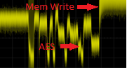
If you look carefully at this logic you can see there are two different execution paths. One where it runs AES and one where it doesn’t. The BitBox02 runs the AES algorithm in software as do many wallets to allow for better audit-ability. However, this makes the algorithm take much longer which makes its power signature more pronounced. This means that if we measure the power consumption, we will see a difference if step 8 runs or step 7 runs. So, the first step of the attack is to detect that AES decrypt didn’t happen (remember light bulb off and still hot).
The next part of the attack is to notice in the code that the counter increment is the final action after checking the password. This means that until that final step executes the MCU has no memory that any attempt was tried. So the attacker just needs to reset the MCU before it increments the failed attempt counter. I implement this attack by directly connecting to the MCU reset line. This gives the attacker a very accurate and fast way to reset the chip. I also inserted a shunt resistor directly inline on the 3.3V power rail. Additionally, I connected a wire to the I2C line controlling the SE. I used this as a trigger to align my timing so I could accurately find the exact place in the power trace I was interested in.
However, these are small signals we are working with so I needed some additional equipment to make the measurements. So I also used a differential probe (from NewAE) to remove the common mode signal (3.3V). Once this was done I could see some interesting data on the scope. But now the challenge was to find the exact place in time where the AES decryption of the seed happened
I used the writes on the I2C bus to the SE to synchronize my power trace with the code being executed. Next, I knew when the MCU writes to flash it would cause a large power spike as well so I was able to find that quickly. So now I was able to bound where I was looking to try and find the signature of AES. And to my surprise the AES difference just jumped out at me without having to do any computer aided processing of the signals (see below).
No AES With AES
Time window
Now I had the position precisely located and I had precise triggers which allows me to reliably reset the MCU just before the code can update the MCU attempt counter (mem write). This allows the attacker to continue to try passwords without the MCU known, but Shift had a backup.
Defense in Depth
Shift implement another security feature specifically to be additional protection in case of an error like the attack above.
When the SE does its part of the key derivation to get what I called the final secret they use a cryptographic command on the SE called KDF (key derivation function). This is just a fancy name for “hash this data with a secret key on the chip”. They actually do this with both slot 3 and slot 4. But slot 3 (ROLLKEY) has an extra bit checked in its configuration on the SE. It has the “LimitedUse” flag set (SE configuration is listed in the source code). This flag has the effect that every time this slot is used with a crypto command (like KDF) it will increment an internal counter in the SE until it reaches its maximum value. Once the maximum value is reached crypto commands will not execute on that slot.
Shift has the counter set such that this slot can only be used 730500 times.
#define MONOTONIC_COUNTER_MAX_USE (730500)
So this provides an upper limit on usage of the BitBox02 to act as a failsafe against brute-force attacks.
Conclusion
In the above I described how the password attempt counter in the MCU can be bypassed allowing an attacker to attempt up to 730500 guesses using the user interface. The above attack I believe can also be developed further to be implemented by just plugging into the device through USB without any disassembly. This attack would use the less precise method of “cutting the power” to cause the BitBox02 to reset before the attempt counter increment. The device would use the power signatures to synchronize the triggers for the attack. Also a device could be constructed that could automate the password guessing by using sensors placed over the capacitive touch electrodes. This would result in a low cost non-invasive attack. However, it would still be “slow” because guesses require the device user interface. If an attacker steals your device he would still need 1-2 months. If the victim notices the device is missing he can move his funds. But to prevent this, the attacker could also replace the stolen device with a “bricked” device. Then the user may just buy a new device and reinitialize with the same seed because they are unaware of the attacker.
Lucky for Shift this error was able to be fixed with a software update. But the important thing to remember when selecting a hardware wallet is all wallets are going to have security issues and if they don't it means no one is looking. The best way to judge a wallet is to look at what was the nature of the past security errors and what was the company’s response when the error was disclosed to them. No wallet will ever be perfect, and they will all make different compromises, but it’s important to use a well-researched wallet so you can know where you stand from a security perspective.
Fixed in versions: bl-harding branch, release likely name
bootloader-1.1.0
Hardware wallets seek to protect your seed words and secure
transaction signing from both remote and physically present attackers.
Creating a design that is secure in the presence of both remote and
physical attackers is an incredibly challenging task. So don’t be surprised
as you see every hardware wallet make its way into the headlines with a newly
discovered security weakness at some point.
In this document I discuss, in an informal way, how I discovered
and went about creating the previously disclosed short PIN attack on the COLDCARD
wallet (CCW). Here is CoinKite's write up on this attack https://blog.coinkite.com/use-long-pins/. The attack is achieved by
connecting a man-in-the-middle (MITM) to the bus the CCW uses to communicate
with its secure element (SE). Then commands on the bus are modified to cause
the MCU to not count failed PIN entry attempts. This gives the attacker
an unlimited number of attempts to guess the PIN. The mitigating factor
is the wallet user interface limits the maximum guess rate to about 10 seconds
per guess. This is still fast enough to easily brute-force
"short" PINs but recovery of longer PINs is not practical as long as
they are random. However, it may be possible to increase this guess rate
of this attack to around 1 second per guess, but it will require some new
unproven methods I'm researching. Currently there are no foreseeable
methods to increase the rate faster than ~1 second without extracting the MCU
"pairing" secret from the MCU flash. So 8 digit PINs are still
pretty safe (multi-year attack required).
Hardware wallet security basics
The purpose of a hardware wallet is to improve the security of
transaction signing and protection of your seed phrase over what a PC or phone
can offer. Hardware wallets attempt to achieve this by creating hardware
and software with less complexity than a PC or phone. This allows a much
more thorough review of all the possible attack vectors by reducing the
hardware and software complexity. Where ever you see design complexity you will
find security vulnerabilities.
Most hardware wallets do a very good job of protecting against remote
attackers. The term remote means attacks where the
attacker doesn't have physical possession of the device. A remote
attacker can manipulate data sent to the hardware wallet or control a device
that the wallet communicates with. This creates limits on what the attacker can
do. If the wallet connects to a computer over USB the attacker needs to
find and exploit a bug in the devices USB software stack or application layer
usage. If the wallet seed phrase is unencrypted in an EEPROM the remote
attacker can't take advantage of that weakness he can only target USB errors.
Remote attackers are limited in what software/hardware they can look for
vulnerabilities in because they can only see exposed external interfaces.
However, there have been some very clever attacks where remote attackers try to
look past these external interfaces by measuring very precisely the timing of
data responses which can give them insight into what the device is doing
internally. But even with great sophistication the attackers are still limited
and hence it is much easier to protect code execution and use of internal
device secrets because there is less software and hardware exposed to attacks.
The hardest challenge for wallets is protecting secrets from a physically
present attacker. This type of attacker can steal your device from you on
the street or from your house when you are gone. They can modify your
device hardware or firmware without your knowledge. Physical attackers
have unlimited attack vectors. All security can be defeated by a physical
attacker if the attacker has enough time and money. For example, labs
have the ability to completely reverse engineer the silicon chip or a
government can force the manufacture to turn over design files. After a
chip's internal design has been fully recovered a lab can very effectively
target specific areas on the chip using a laser to induce changes in memory or
logic. It is possible to discover
sensitive areas by testing randomly but can take a long time and may be too
complicated to discovery by random trial. The memory state change can
cause the chip to not check critical security parameters before running some
operation. No device is secure against physical attacks, but some devices
require the attacker to spend much more time and money. So, when discussing physical security, it
should always be discussed in terms of estimated dollars and time to break the
security. The goal of the hardware wallet designer is to implement
security features that have a low implementation cost but result in a very high
cost to an attacker, I'll call this an asymmetric defensive measure.
The first level of asymmetric defensive measures is commonly achieved by wallet
designers by requiring the user to enter an authorization PIN before the wallet
will sign any transaction. Only after the PIN is entered will the wallet
sign a transaction which additionally requires approval by a physically present
user's button press. However, PINs are relatively short in order to make
it easy for a human user to remember and type. So if PIN entry attempts
are not rate limited by the device in some way a computer can quickly guess all
the possible PINs. The common method of rate limiting is for wallet
software to keep track of failed PIN entry attempts in non-volatile memory and
add an increasing delay before it accepts the next attempt. In principal this
is very effective and can make even a 4-digit PIN secure with the appropriate
limits. The COLDCARD Wallet uses these methods in their design which will be
discussed in more detail next.
COLDCARD wallet security
The COLDCARD wallet is a
product developed by Coinkite Inc. It includes a secure element (SE) for
storing the secret seed / key, authenticating firmware updates, and activating
the genuine LED. A secure element defined in this embedded context
is a device designed to provide secure computation or and cryptographic
services along with secure data storage. These devices act as a companion
chip to a main processor so the processor can off load the security critical
operations to the secure device. These low-cost devices can increase the
physical security of a design because they are specifically designed to protect
from various physical attacks such as power glitch attacks. However,
using a SE adds complexity to the design and mistakes either in system architecture
or usage can be made that create security holes.
There are lots of strategies used by different hardware
manufactures when designing security architectures for wallets. The
Trezor team chose to create a simple hardware design with no secure element and
just use a general purpose MCU. The Ledger team chose to add a secure
microcontroller (MCU) as a co-processor (a secure element) to manage
transaction signing and protect the key. In theory the Ledger should have
a higher (more cost and time required by an attacker) security level than the
Trezor, but in practice it is not clear which has better security, and many
believe the Trezor to be more secure. These opinions come from analyzing
the discovered attacks on each of the devices. The SE element in the
Ledger uses an exposed bus which creates many opportunities for
man-in-the-middle (MITM) attacks that are hard to engineer around. Additionally,
the SE used in the Ledger requires wallet developers to write and load custom
code, but the chip manufacture's licensing requires it to be closed source (so
I have been told). These aspects of using this SE increase the attack
surface and reduce the quantity and quality of testing of that surface. However, these additional risks have to be weighed
against the risks of using just a general purpose MCU to store device secrets
like in the Trezor which is more susceptible to physical attacks.
Coinkite uses a slightly different approach from both the Trezor
and Ledger. The COLDCARD wallet uses a
different style SE (ATECC508A). The device used is publicly available and
it is a fixed function device. Users cannot modify the device’s APIs or
function. Users can only configure the access permissions for the
different storage areas and those configurations are always public. Information
on this SE is also more publicly available than the Ledge's SE (STM31 family
secure MCU). Additionally, it also
benefits from security economies of scale because the CCW SE is fixed function. All customers buying this chip use the same
APIs so the device receives the benefit of the accumulated testing of all
customers. Plus many customers pay third
party labs to analyze the chip independent from the manufacture. This allows for an accumulation of confidence
in the device’s function. However, this
SE does not support the bitcoin secp256k1 curve internally so CCW is just using
it as secure non-volatile storage for the key. The bitcoin cryptography
is actually preformed in software on the host MCU after the key is securely read
from the SE.
The reason to store your key in a SE is to increase the protection
of the key from physical attackers. It
also helps protect against remote attackers, but the larger improvement is the
protection from physical attacks. General
purpose MCUs (like the STM32 use in the CCW) are very weak against physical
attacks and most people don't realized how weak. Here is an example from
a website advertising reverse engineering services to read out the flash
contents of some MCUs.
If you search the internet you will see lists of thousands of MCUs
that can have their firmware extracted. Also, just because you don't see
a specific part listed in your online search does not mean it is not
vulnerable. If you look at the number of devices on these lists that span
many manufactures, you realize it is very likely any general purpose MCU can
have its entire memory contents read out for ~$2000 USD or less. In the
case of a hardware wallet $2000 is not much of a deterrent to an
attacker. Adding a SE element is an asymmetric defense because it can
massively increase the difficulty and cost for an attacker. This is
because SEs are designed with the sole purpose of protecting against physical
attacks. So, in general, vulnerabilities in SEs are much fewer and more
difficult to exploit than general purpose MCUs. It is hard to estimate
the cost to an attacker because there are few public attacks, but I would
expect on average orders of magnitude more difficulty and cost. So I
wanted to see if the COLDCARD wallet was effectively using their SE to achieved
this higher level of security (increasing difficulty and cost of attacks) or
were there some mistakes that actually weakened it security.
Attack step by step
The secure element used in the COLDCARD wallet is the Microchip
ATECC508A. No research was needed to figure this out because they promote
this on their website. The first thing I did was to spend some time
reading through website documentation to see how the CCW was using this
device. One nice thing about this SE is that the datasheet is fully
public here. After reading some user
documentation from the COLDCARD product page one thing caught my
attention. In the advanced topics section "PIN
codes and the security element" the documentation described how PINs are used in the
device. What I noticed was that the CCW stored PIN hashes on the
SE. My first thought was I might be able to directly brute force the PIN
on the SE bus which would bypass the MCU software timer limits if the designers
hadn't been careful. So I went to the code on github to
see some more details.
The software was well organized, so it didn't take long to find
the things I needed. First, I did a general survey of the directory and
file names and I came across a file called pin.cunder the stm32/bootloader directories.
It was hard to get a complete picture of how the SE was being used without
knowing the exact configuration of the SE chip, but this was easy to
find. This is public information right in the code in a file named ae_config.c.
It’s painful to decode these configuration bytes manually, but
there was also a python script included in the CCW code base that gives you
some text descriptions. However, I had a JavaScript tool that the SE
manufacture provided that can directly decode C array style chip
configurations. So just needed to add some padding bytes and paste it in
to the tool. This image below is from the tool which decodes the
configuration bytes in to a nice human readable format. I manually added
in the descriptions base on CCW documentation.
This really helps visualize what is going on with the SE.
Well it helps once you are familiar with the device. Don't be worried if you don't understand this
right away 😊.
Let me give you a quick crash course. A slot is an area of storage on the
SE that can have individual security permissions attached to it. There
are three important slots used to read out the secret key: Slot 9 (the secret),
Slot 3 (the PIN hash), Slot 1 (a shared secret stored in the MCU). In
order to read slot 9 you need to know the value in slot 3 (this requirement is indicated
by ReqAuth
and AuthKey
fields). In order to use slot 3 you need to know the value in slot
1. To authorize a slot for use you need to run the CheckMac command on the
SE. This command requires the MCU to prove knowledge of the value in a slot by
providing a correct MAC (message authentication code) response to the SE's
challenge. Then the SE returns success or fail and sets the internal chip
state. The pseudo code logic flow goes like this:
CheckMac(slot 1);
Ask user for PIN;
CheckMac(slot 3, <user
PIN hash>);
Read(slot 9 using slot 3 as
the decryption key);
When I was first thinking through this I thought I was going to be
able to skip the MCU rate limit by stealing a CheckMac(1) that was
being used for something else and then substituting my own guess at the PIN in
slot 3 by sending the PIN hash in a CheckMac command. The result
returned by CheckMac(3, <pin hash>) would tell me if my guess was
correct. However, I missed a basic aspect of the design which was the
value in slot 3 is not just the hash of the PIN alone but includes the
"pairing" secret (in slot 1) as part of the hash which only the MCU
and SE know (I don't know it). This meant I couldn't directly brute force
the PIN with this method. So I had to keep looking.
I reviewed the documentation further and found a new angle of
attack. The documentation indicated that the PIN attempt counter is
located on the ATECC508A (SE). I immediately wanted to investigate how
that counter was protected. In pin.c in the function pin_login_attempt() I found a call to ae_get_counter() which reads
and increments the counter. In ae.c I found the definition of ae_get_counter() and saw that
it called the command OP_Counter (0x24)
on the SE. So I pulled up the SE datasheet to double check how the
command worked.
The important thing to note in the above command is that the value
returned (Output Parameter) by this command is not authenticated. It is
just plain text on the bus. This allows an attacker with
physical access to control the value of the counter. It is possible
to authenticate the counter state on the SE, but it requires additional
commands which were not being used at the time. So at this point it
appears the attacker can have total control over the read counter value.
This allows the attacker to bypass the MCU failed attempt counting which allows
PINs to be tested at the maximum rate allowed by the MCU boot loader. At
this point the attack appeared to be fully achievable, but theory can be
different from reality, so I decided to move to testing on a real device.
Then I ordered my first COLDCARD Wallet. Once I received it, I verified
the boot loader version matched what I had been reviewing and it did.
Next, I needed to open the plastic case so I could access the
internal circuitry. A simple screw driver did the trick. There was
no need to be careful 😊.
Once it was opened, I needed to identify
which chip was the secure element. I used the SE's datasheet to get the
dimensions which quickly narrowed it down to just once device, U4.
Now that I had identified the SE I needed to determine which pin was the single
wire interface. The chip can be communicated to using standard UART
communication with a start bit, eight data bits and a stop bit @ 230400
baud. The datasheet specifics that pin 5 is the SWI pin, but there are no
markings to determine if pin 5 is in the upper corner or the lower
corner. So I needed to probe with a multi-meter to discover the power and
ground pins in order to determine which orientation it was in. After
probing I determined that pin 5 was in the upper left-hand corner.
Now that I had identified the chip and
communication pin it was time to tap into the communications. The end
goal of the attack is to intercept communications from the host MCU and modify
them (if required) before sending them to the SE and also the other way around.
To do this the communication line between the SE and host MCU needs to be
cut. Then each side needs to be connected to the attacking MCU so it can
act as a MITM. In general cutting traces is a pretty easy task, but you
have to make sure not to drink too much caffeine when they are small like
this.
So I put down my red bull and took off my hoodie and got out my
trusty razor blade and carefully cut the trace coming from pin 5. The
best method is just to press and twist at it one pass at a time until you see
the copper break. If you look closely at the bottom arrow you can see
that the copper is cut through and is exposing the FR4 below. If you look
at the upper arrow you will you can see some more copper. This is a
ground or power plane I accidentally cut in to. Cutting in to it wasn't a
problem, just had to make sure no copper flakes bridge the gap.
Now that the trace was cut, I needed to connect some wires to bring
those signals back to my attack MCU. The bottom wire actually broke off while I
was messing around with it to get some pictures, but lucky for me that wire is
really easy to solder because there is a via (hole to bring signals to other
layers) that the wire could be soldered. The top trace didn't have any
via to help with soldering. The only exposed conductor on that net is at pin
5 on the SE. However, the pin is very small and difficult to
solder. So I decided to just scrape the solder mask off the trace with my
razor blade and solder right to the trace. To do this you lightly scrape
across the trace and repeat until you see enough copper exposed to
solder. I soldered on a couple more wires at other locations to get power
and ground and now I was ready to start reading some bytes.
It was time to connect my attacking MCU. I chose the
Microchip ATSAME54 development kit for this attack. This is a 120MHz
Cortex M4, but this attack doesn't really require any special features except
two UARTs and enough speed to process the received packets before the host MCU
notices something is wrong. So almost any MCU would work, but this was
just one I was familiar with.
The first task I decided to do was to just snoop the bus and
decode the packets to a human readable form. So I just shorted the two
wires by attaching them together and connected to my MCU UART pins. Then
I used an example project that reads the UART to get started. The SE
sends data in an encoded format where bytes represent bits. This adds a
little bit of work to decode the signals, but not too much. The encoding
works like this: 0x7F and 0x7E represent a 1 and other values represent a
0. I believe the reason for this is to allow for larger differences
between the MCU clock and the SE clock since the SE does not have an accurate
clock source. It appears the SE tries to calibrate its clock using the
MCU's transmission because the receive tolerance it relatively tight 4.1us -
4.56us bit time, but the response tolerance is massive 4.6us - 8.6us bit
time. In my design the bit time I saw from the SE is 6us (which is listed
as typical in the datasheet). Below is an example of a transmission from
the MCU to the SE.
The above represents binary 1,1,1,0,1,1,1,0. The least
significant bit is sent first so this corresponds to the value 0x77. If
you look at the SE datasheet you can see this is an expected value that
indicates a command sequence is coming next.
If you review the datasheet you will see that next comes a byte
count byte followed by the command opcode and parameters bytes. Decoding
these packets was straight forward. I used a timeout between UART bytes
to indicate a transmission was complete. In the trace below you see some
bytes on the left sent by the MCU. Then you see a delay (where my timeout
would trigger) and then the bytes on the right are the response from the
SE. You can identify the bytes sent by the SE because they have some
delay between each byte. This type of analog signature is used by some
very advanced attacks on other systems where measuring subtle analog properties
of WIFI RF you can get a lot of information about a device's internal data.
Once a transmission was complete, I just parsed the received bytes
to find the opcode and a couple parameters. See the example output from
my parser below.
The first line to the left shows "CMD: R 28" which
indicates a read on address 0x28. Address 0x28
corresponds to slot 5 which is the "last good" slot. The line you see
below the read command is the response from the SE (byte count byte (0x07)
then data (0x7d, 0x00,..) then crc (0x35, 0xb5)) which indicates I have
entered my PIN code 125 (0x7d) times during testing and
development of this attack. The next line is a counter read which also
returns 0x7d which is equal to slot 5 which means there currently no
failed PIN entries. So once I started getting some human readable
information out I went back to the code and tried to match up the sequence of
commands on the bus to the sequence I expected the code to execute. If we
skip to the last couple line you see "CMD: Check 07" which means the CheckMac
command run on slot 7. Slot 7 is the duress PIN slot and then the next
command is a Counter command in mode 1 which means to increment the
counter. If we look through the expected code you can find this sequence
below in pin.c in
the pin_login_attempt() function.
Remember this counter command is key to implement the hack.
The ae_get_counter() function
gets the newly incremented counter value. The attempt_target variable was
previously calculated by reading the counter and adding 1. If you pass
the check then the is_real_pin() function
(below) tests the PIN entered which is the goal of the attack. The
response to the CheckMac(3) can be seen on the bus so we know if the entered
PIN was a match right away.
The code that I specifically
want to attack is in pin_setup_attempt()(see
below). The num_fails variable
is what tells the boot loader how many failed attempts there have been.
The goal is to make "count -
last_good" line 463 equal 0. There are actually a
couple ways to make this happen. We can fake the last_good read (also not
authenticated) or the counter read or both. I actually chose a slightly
different method which was to block the counter increment. This method
seemed easier because it just required a static replacement of the counter
command mode 1 (read and increment) with a counter command mode 0 (read only)
and no other modifications to bus traffic.
So now that I'd confirmed that the code was matching the actual
bus traffic decoding, I was ready to start implementing the real attack code to
modify the bus traffic. The architecture of my code was to act as a UART
byte forwarder. When the MCU sent bytes on UART1 I would decode the bytes
and check which command it was print it and forward those bytes to UART2.
UART2 is connected to the SE. When the SE responded on UART2 I would
forward the response back to the MCU on UART1. Initially this seemed
really easy, but some issues quickly popped up. First, I discovered the
host MCU had a timeout on some commands that was too short for me to receive
then forward and send back the response. Luck for me this was another
command sequence that I could fake with just a static response back to the
MCU. But then I noticed it wasn't just that static command that had this
issue, it was all the commands. So I
looked in to this closer.
The SE waits to be polled by the MCU before responding to
commands. For example, the CheckMac command the datasheet shows
it can take up to 13ms before the SE has the data ready. So the COLDCARD
MCU waits 13ms and then sends a "transmit" request (0x88) on the
bus. Then the SE needs to respond fast in a max of 130us (micro
seconds). So this is what was causing me issues. The CCW MCU had a timeout for that response
that was in that range. What I decided to do was to add some intelligence
to my code. The host MCU was waiting the max timeout period before
polling the SE with the 0x88, but that timeout is the max. In most
cases the SE has the data ready before the max timeout. So I added some
logic for my attack MCU to start polling the SE earlier and just save the SE's
response and wait for the host CCW MCU's 0x88 and then send the buffered
response.
Now things were working pretty good, but I noticed a couple more
things that needed to be adjusted to make the attack practical. The first
thing I realized I had forgotten about was the brick-me PIN. Entering
this PIN will cause the MCU to send a command to the SE that destroys the value
in slot 1. The value isn't actually destroyed, it is just changed using
the DeriveKey
command on the SE. It is possible to record both random numbers (the
command parameters) that appear on the bus before the DeriveKey command is
issued. Then later we could learn the
pairing secret from the MCU. We can then
recover the SE secret still by deriving the same new slot 1 value
externally. But there is a much easier way to deal with it which is to
just block the DeriveKey opcode. So in my code before I forward bytes to
the SE I check to make sure it is not a DeriveKey command. This
protects from accidentally bricking the device when searching for the user PIN.
The last thing was to bypass some additional rate limiting in the
code. The CCW starts indirectly applying additional limiting after 10 PIN
attempts per power cycle. At 25 attempts it requires a reset. The
counter for this limit is stored in the MCU RTC (real-time clock) backup area
(ram) that is only lost on a power cycle. This was a little tricky to get
around, but I noticed the counter is reset right after a valid PIN (see below).
The upper arrow (line 573) is where the PIN sent to the SE to be
tested for correctness. This function uses the CheckMac command to test
the PIN. If you remember back we discussed that the CheckMac command returns
success or fail and then records the state internally to unlock other
slots. But just as with the Counter command the return value from CheckMac
is not authenticated. So the attacker can change this response. The
attacker cannot change the way the internal state is set, but we can change
what the MCU thinks happened by changing the response to "success"
when it was "fail". This
causes the next line to execute at the lower arrow (line 582) which resets the
MCU internal RAM counter. The code that runs after this line expects slot
3 to be "unlocked". This code fails, but it fails in an
expected way "EPIN_AUTH_FAIL". So it only causes the MCU
to return back to the PIN entry screen and lets us try again.
One interesting thing that I came across in the code part way
through the development is that the CCW developers were aware of the potential
of counter spoofing. In the below code see the comment on line 329.
When determining the overall security of a
product it is important to determine the root cause of previous errors.
The above comment describes the fix for the attack I preformed almost
exactly. So the question is why was the code still released even with
this known vulnerability? I have to play the speculation game but here
are a few possibilities:
1. They thought PIN rate limiting
was backed up with the MCU RAM counter good enough
2. Didn't consider the attack
significant because the difficulty was to high
3. Didn't consider the attack in the
context of device theft
4. Didn't consider automation of the
PIN entry GUI
I believe it may be a combination of a few
things, but I think largely it is number 2 and 4. There were a couple
occasions where CCW team members made suggestions or comments regarding the
difficulty of physical attacks. When I first contacted the support line
it was acknowledged, ~"you might be able to do this MITM attack, but
because of the CCW physical design it will be hard". Also shrinking
and hiding traces came up again when they fixed the issue as an additional
mitigation method. I agree mitigation is good, but the hardware
modification part of this attack only took me ~30 mins and making PCB traces
smaller and hiding them might increase the time to 1 hr at most. So, it
is not a good use of resource time (not an asymmetric defense) unless you go
much further. In general, I don't think physical accessibility of
circuits should be considered as part of your system security unless you go to
the extreme. Extreme is maybe one-inch thick epoxy covering everything
with all die bond mounted components. That doesn't stop an attacker, but it
turns hours of work into weeks of work and that time allows a user who lost
their wallet to take action.
Conclusion
In summary here is a quick review of the
CCW security pros and cons from a high level.
Pros:
1.It is completely open source
software.
2.The software focuses on a limited set of
features (just Bitcoin).
3.Both the MCU and secure element are
publicly available and have public full datasheets.
4.The code is organized and thought
out.
5.The team responded quickly and
professionally when the attack was disclosed.
All of these combine to make the product
anti-fragile. Meaning mistakes are easy to find and the code is
structured to make things generally easy to fix which allows the product to
improve rapidly over time. However, there are some negatives.
Cons:
1.The boot loader cannot be updated. This
is a trade off since an update-able boot loader is also a security risk, but in
my opinion the boot loader is preforming too many features (increased risk of
errors) to not allow for its updating which is what makes the short PIN attack
more significant.
2.I think there seems to be an opinion in
the company that hardware attacks are “difficult”, so they are less of a
worry. Now I may be a little biased, but I believe this thinking can
cause them to overlook things similar to the short PIN attack.
3.The use of a shared pairing secret between
the MCU and SE (Slot 1 value) causes the security level to be reduced to the
same as the MCU flash (little security benefit from using the SE).
Meaning that if I can somehow extract the MCU flash then I can recover all the
information from the SE because the PIN can be brute-forced at the maximum SE command
speed (~10ms per guess, 8-digit PIN can be guessed in ~10 days). Note, this was not an attack I achieved but
something that may be possible due to the general weakness of MCU flash to
physical attacks that was discussed earlier. I have made a suggestion to
Coinkite on how using a different variation of this SE could allow for the
pairing secret to be eliminated, but it will require significant changes in the
software.
The important thing to remember when
selecting a hardware wallet is all wallets are going to have security issues
and if they don't it means no one is looking. The best way to judge a
wallet is to look at what was the nature of the past security errors and what
was the company’s response when the error was disclosed to them. No wallet will ever be perfect, and they will
all make different compromises, but it’s important to use a well-researched
wallet so you can know where you stand from a security perspective.